Fisica a Ferrara: orientamento didattico
Condensed Matter
Condensed Matter
-
Condensed Matter
This track aims to give to the student a solid understanding of material properties at microscopic and macroscopic levels, encompassing two sub-tracks: Magnetism of Nanostructures and Semiconductor Physics. The topics range from those relating to fundamental properties of these structures, treated within the framework of Solid State Physics, to the experimental investigation and applications.
| Course | Sugg. | SSD | Att. | Table | CFU | Sem./Anno |
| Advanced electromagnetism (not active in 20/21) | FIS/01 | B1 | I | 6 | I/1 | |
| Electron microscopy: theory and applications | M/S | FIS/01 | B1 | I | 6 | I/1 |
| Introduction to particle accelerators and detectors | FIS/01 | B1 | I | 6 | II/2 | |
| Object-oriented programming for experimental data analysis | FIS/01 | B1 | I | 6 | I/1 | |
| Physics of electronic devices | FIS/01 | B1 | I | 6 | I/1 | |
| Semiconductor physics laboratory | M/S | FIS/01 | B1 | I | 6 | II/2 |
| Solar energy systems | S | FIS/01 | B1 | I | 6 | II/2 |
| Magnetic properties of matter and laboratory | M | FIS/03 | C | II B | 6 | I/2 |
| Sensors: physics and technology | S | FIS/03 | C | II B | 6 | I/1 |
| Surface physics and nanostructures | M/S | FIS/03 | C | II B | 6 | I/1 |
| M: Strongly suggested for the sub-track Magnetism of Nanostructures S: Strongly suggested for the sub-track Semiconductor Physics |
| Research Group |
| Diego Bisero |
| Lucia Del Bianco |
| Loris Giovannini |
| Vincenzo Guidi |
| Cesare Malagù |
| Federico Montoncello |
| Federico Spizzo |
| Melissa Tamisari |
| Donato Vincenzi |
| Laura Bandiera (INFN Ferrara) |
| Andrea Mazzolari (INFN Ferrara) |
Condensed matter program
The Condensed Matter track aims to give to the student a deep understanding of the matter that makes up most of the things which surround us every day, from both theoretical and experimental point of view. It concerns the study of the things in between very small (Nuclear and Subnuclear Physics) and very large (Astrophysics). There are three common courses, Electron microscopy: theory and applications, Semiconductor physics laboratory and Surface Physics and Nanostructures. They provide a general introduction and are of service to both subtraks described below. The course Surface Physics and Nanostructures offers a general view of all the main issues concerning the Physics of Condensed Matter. It presents a wide introduction of the physical phenomena at surfaces, interfaces and at the nanoscale, and addresses current topics like photonic crystals, plasmonics, magnonics and graphene, under both theoretical and technological perspectives. Fabrication methods are also presented together with the most advanced measurement techniques (in the fields of microscopy, diffraction, and spectroscopy). The Condensed Matter track contains two sub-tracks: one, Magnetism of Nanostructures, devoted to the study of magnetic properties of surfaces, interfaces and nanostructures; the other, Semiconductor Physics, deals with semiconductor applications such as sensors and photovoltaic cells.
The Magnetism of Nanostructures sub-track has a Fundamental Physics formulation, with some applications. Here you can find courses where the magnetic properties of matter are explained, based on the elementary magnetic interactions between atoms (Magnetic Properties of Matter and Laboratory). Such interactions are strongly influenced by the spatial arrangement of atoms and therefore the geometry of the samples plays an important role. In particular, the reduced dimensionality and the reduced dimension are important. These studies can then converge either in a theoretical thesis work, concerning the development of models and corresponding numerical simulation programs or an experimental work, to be carried out in our laboratories.
The Semiconductor Physics sub-track is mainly oriented towards applications. In the course Sensors: Physics and Technology the fundamental aspects of semiconductor-metal and semiconductor-gas interfaces are deepened and applied to the nanoscale. Solid state gas sensors applications are then explored, with particular attention to environmental applications and diagnostic ones. The course Solar Energy Systems introduces the fundamental physics of photovoltaic devices and the technology of manufacturing of silicon and thin film PV. Different approaches to exploit solar energy will be presented, ranging from concentrated solar power (solar to thermal and electrical energy), to direct solar to fuel conversion, to photobioreactors using natural photosynthesis for CO2 capturing and biofuel generation. Finally, the Semiconductor Physics Laboratorycourse provides an insight in the worldwide mostly used techniques for characterizations and machining of semiconductor materials. The laboratory activities are performed in a fully equipped clean room, training the student to operate in a very peculiar and technological environment. Activities are focused on high-resolution x-ray diffraction, optical photolithography, white light and infrared interferometry.
In Solar Energy Systems peculiar applications related to and devices for converting solar energy are developed. Different ways of use of solar energy, ranging from conversion to thermal or electrical energy to bioreactors based on the use of natural photosynthesis for energy storage are presented.
Despite this large variety, there is a common thread to Condensed Matter Physics: the understanding of the collective behavior of systems which consist of large numbers of constituent elements. Such collective behavior often turns out to be very rich and complex.
Career possibilities
The employment opportunities in the Condensed Matter track are mainly addressed towards scientific research, i.e. towards universities and research institutions, and the industry, in particular in the sector of innovative technologies. Also some opportunities are provided by the startups that were activated as spin offs of our Department.
Condensed Matter research groups
Semiconductor and sensor laboratory
The Sensors Laboratory in the University of Ferrara carries on studies and manufactures gas sensors based on semiconductor oxides, for applications in the environmental, agro-food and medical fields. To detect the presence of gas markers it is necessary to maximize the specific surface, and therefore nanostructured semiconductor oxide powders become suitable materials to produce sensors with that aim. The theoretical study on the nanostructures’ properties of the gas-semiconductor interface phenomena is dealt extensively from both an analytical and numerical point of view. The entire development process of the device is also developed at the laboratory. The equipment and interdisciplinary skills available to the laboratory allow the preparation of nanostructured powders and screen printing pastes, as well as the complete morphological-structural characterization of them (thermal analysis, XRD, SEM, TEM). Sensors made using thick film technology are then electrically characterized in flow-regulated climatic chambers.
The control electronics are also designed and manufactured in the laboratory.
A university spin-off allows the large-scale production of devices in the form of sensor arrays in control units equipped with an electronic data acquisition and transfer system. Finally, software for online monitoring of these control units was developed.
One of the most solid realities in collaboration with the laboratory is the startup SCENT S.r.l., an award-winning company (Marzotto Group, LILT, regional POR-FESR plan and Chamber of Commerce of Ferrara are among the entities recognizing the value of the company over time) operating in the field of cancer screening, and holds two patents for medical diagnostic instruments. SCENT S.r.l. has an ongoing research agreement with the Department of Physics and Earth Sciences, and uses nanostructured chemoresistive sensors for the operation of its devices. In particular:
- SCENT A1 device (European patent number #: 3210013) is aimed at the early screening of colorectal cancer, alongside the already existing FOBT diagnosis, and is currently in the multicenter certification phase, before arriving on the national market.
- SCENT B1 device (National patent number #: 102015000057717) is currently used for research purposes to monitor the production of volatile metabolites from cell cultures, and to monitor the development of relapses and metastases in the post-operative setting on cancer patients.
The Laboratory collaborates with industries (SACMI) and other research groups in Italy and Europe, also in the context of national and international projects.
Synchrotron Radiation on graphene devices – Nanomagnetic logic – Stripe domains reorientation in ferromagnetic films
Synchrotron Radiation on graphene – The aim of the activity is to apply the high sensitivity of Near Edge X-ray Absorption Fine Structure (NEXAFS) combined with Resonant Soft X-ray Reflectivity (RSXRR) spectroscopy, obtained by Synchrotron Radiation, to the context of integration of graphene into the planar silicon technology. The measurement capability is explored to analyze the impact of transfer approaches, taking into account the effect of defects in the graphene film and their correlation with the device electrical behaviour.
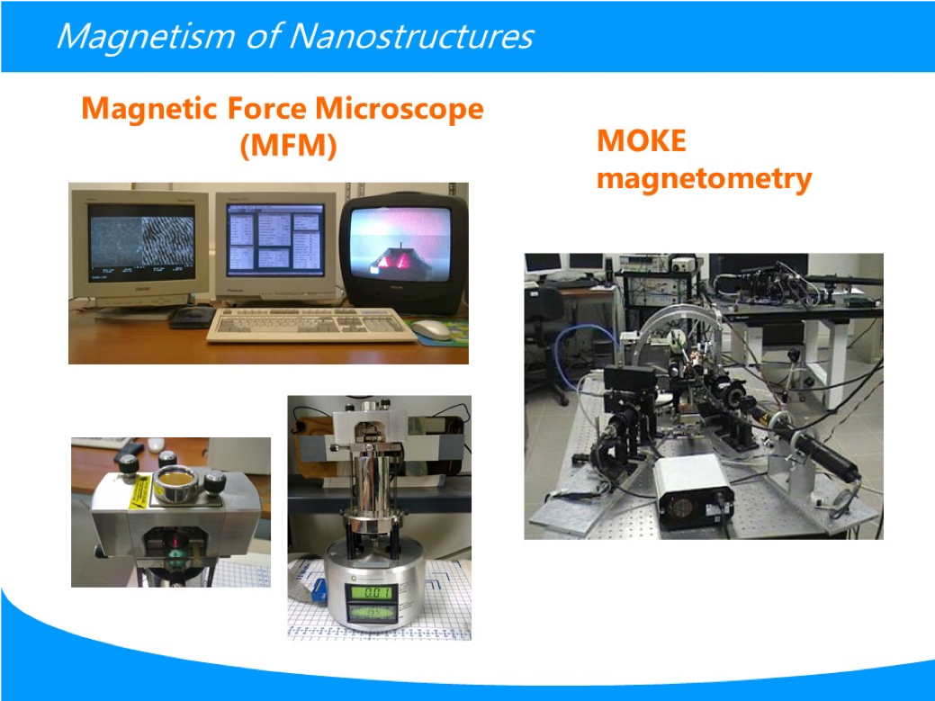
Nanomagnetic logic – The research activity is devoted to the investigation of the magnetization reversal of a majority gate consisting of dipolarly-coupled magnetic nanodots. A combination of magnetic force microscopy (MFM) and magneto-optical Kerr effect (MOKE), assisted by advanced micromagnetic simulations, is used to investigate the robustness of operation and the tolerance to the misalignment of the clocking field.
Stripe domains reorientation in ferromagnetic films with perpendicular magnetic anisotropy – The research activity is devoted to the experimental investigation by Scanning Probe Microscopy (Atomic Force and Magnetic Force Microscopy) together with MOKE magnetometry of the peculiar phenomenon shown by weak stripe domains in a thin ferromagnetic film when a dc magnetic field is applied in the film plane along the direction perpendicular to the stripes axis: namely, the stripe domains reorientation taking place abruptly, above a threshold value for the transversal field. The PMA gives rise to weak stripe domains, which can be directly visualized at remanence by magnetic force microscopy (MFM).
Experimental Nanomagnetism
The research activity of this group deals with the study of the properties of magnetic nanostructures, i.e. systems structured on the 1 nm – 100 nm scale in at least one spatial dimension. When the size of a magnetic material is reduced and gets comparable to the magnetic ordering correlation length, which is in the nanometer range, new and amazing magnetic effects appear. Magnetic interactions, i.e. exchange and dipolar interactions, may also strongly affect the magnetic properties of the nanostructures. In summary, magnetic nanostructures are novel systems where both size/shape and magnetic interactions represent new degrees of freedom that allow to tailor their magnetic behavior. The nanostructures we are presently studying are in the form of nanoparticles and thin films.
Magnetic Nanoparticles – Magnetic nanoparticles (NPs) are generally embedded in a solid matrix, chemically or magnetically different, or dispersed in a fluid, thus giving rise to nanocomposite systems or to ferrofluids. Depending on their structure, composition and magnetic behavior, they can be employed in a large variety of technological sectors: electrical and thermal engineering, magnetoelectronics and spintronics, magneto-optics, catalysis, sensors. Particularly relevant are the applications in the biomedical field where magnetic NPs can act as contrast medium for magnetic resonance imaging, be employed in the production of biocompatible magnetic materials for tissue regeneration, be used as drug carriers and for magnetic hyperthermia. The latter is one of the most studied phenomena from a physical point of view and consists in the production of heat by magnetic NPs subjected to an alternating magnetic field due to hysteresis losses. The effect can be exploited in the treatment of cancer since the heat produced by NPs delivered at the tumor site can raise the local temperature, thus inducing the death of the tumor cells, through the non-invasive application of the magnetic field.
We have large expertise in the magnetic study of NPs systems with special reference to the hysteretic magnetic properties and their thermal dependence, magnetic relaxation processes and magnetic interactions effects, also in relation to the compositional characteristics (both of the NPs and of the matrix/fluid in which they are dispersed) and to the structural features (size distribution, crystallinity, aggregation state). This is crucial in order to optimize the NPs systems for specific technological applications. For this research line, we use SQUID magnetometry, Mössbauer spectroscopy, calorimetric and thermogravimetric analysis.
Thin films – Nowadays, thin ferromagnetic films (FFs) or multilayers have a widespread application in many different fields, both as sensors, e.g. to detect magnetic fields, mechanical stresses, molecules, and for data recording and storage, both in hard–disks and magnetic–RAM memories. In particular, ferromagnetic multilayers are largely employed in the field of spintronics, or spin electronics, where the spin of the electron, and not its charge as in electronics, is the information carrier.
We have good expertise in the production of thin films by sputtering, with special reference to exchange coupled systems (i.e. ferromagnetic/antiferromagnetic bilayers) showing magnetic effects exploited in magnetoresistive sensors (spin–valves) and memory cells.
Regarding magnetic memory cells, one of the important aspects to consider is the energy cost for writing information, that is to flip their magnetization. The use of a magnetic field is effective, but quite energy consuming; alternatively, a spin-polarized current may be used, through the spin-transfer torque effect. Recently, a new perspective has been introduced by the opportunity to couple magnetoelastic FFs, that orient their magnetization depending on mechanical stresses, with piezoelectric (PE) thin films, where the application of an electric field induces a mechanical strain. In this way, when the PE/FF coupling is obtained, the FF reorientation process may be induced through the application of a voltage to the PE thin film.
We are presently investigating this kind of systems, focusing in particular on the effect of the voltage on the magnetic properties of the FF. In this field, our expertise regards thin films production and characterization, from the magnetic, magnetoresistive and structural point of view. For this research line, we use magnetron sputtering, SQUID and MOKE magnetometry.
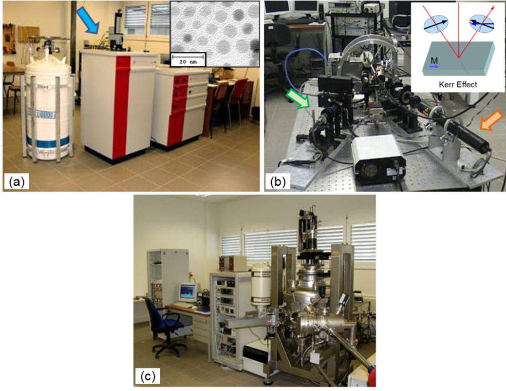
(a) SQUID (Superconductive quantum interference device) magnetometer (indicated by the blue arrow); at its right, the cabinet with the control electronics, at the left, the dewar with liquid helium. The instrument is very versatile and allows the magnetic study of both solid and liquid samples; it is particularly suitable for the study of magnetic nanoparticles such as those shown in the inset (image obtained by transmission electron microscopy). (b) MOKE (Magneto-optical Kerr effect) apparatus; at the right (orange arrow) the laser, at the left (green arrow) the optical devices to detect polarization variations. In the inset: brief description of the Kerr effect. (c) High vacuum sputtering apparatus equipped with one RF and three DC sources. The thin film production takes place in Argon atmosphere; during the deposition process, the sample holder can be rotated, cooled or heated and a static magnetic field may be applied to the sample.
Theoretical magnetism
The Theoretical Magnetism group aims to promote and support the physical understanding of magnetism, magnetic materials and spintronics, with special attention to nanostructured materials. Research in magnetism is broad ranging from computational magnetism to the development of theoretical models aimed at interpreting spin modes and spin waves in different magnetic systems. The systems investigated by this group include nanoparticle arrays of various shape and size, strips, magnonic crystals and quasi-crystals. Such systems evidence several interesting physical phenomena: spin wave propagation or blockage, phase transitions, light scattering cross section, geometrical frustration, effect of random geometrical variation.
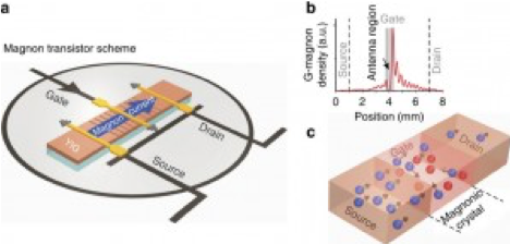
Possible use of spin waves for the realization of a magnonic crystal transistor.
The Sensor and Semiconductor Laboratory
The Sensor and Semiconductor Lab is composed of three different laboratories:
- Sensor LabSolar
- Energy System LabCrystal
- Channeling Lab
The Sensor and Semiconductor Lab have available different settings:
- Clean Rooms, composed of three labs dedicated to chemical synthesis and deposition of nanostructured sensing materials, X-Ray Diffraction analysis on crystals, micro-machining production via photolithography equipped with nano-imprint technology, Low pressure chemical vapor deposition (LPCVD) technology
- Sensor Lab
- Interferometry Lab
- Crystal Manufacturing Lab
Sensor Laboratory
The Sensors Laboratory carries investigations on all key aspects regarding the study and implementation of gas sensors:
- synthesis and deposition of innovative sensing materials, such as organic-inorganic hybrids and non-oxide semiconductors, but also the deepening about new properties of the well-known metal oxides;
- morphological (SEM), structural (XRD), chemical (EDS), thermal (TG-DTG) and electrical characterization of the sensing materials, together with theoretical studies by Density Functional Theory simulation on materials arrangement and their interaction with gaseous molecules;
- study of avant-garde applications for gas sensors, such as medical diagnosis and precision farming, and their integration on technological platforms (i.e. Internet of Things).
The entire development process of the devices is carried out at the Department. The preparation of nanostructured powders and screen-printable sensing films are performed in controlled Clean Room environment.
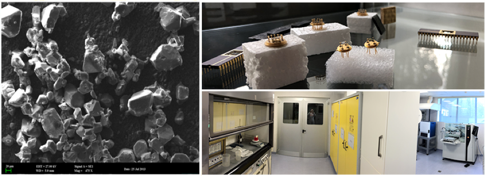
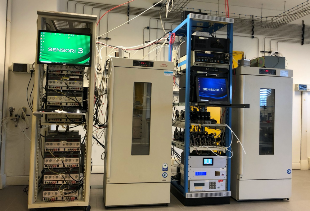
The device’s packaging and the electrical characterization are developed in Sensors Lab, which arranges three test climatic chambers dedicated to flow-regulated exposure to target gases.
Fourier-transform infrared spectroscopy (FTIR) and Diffuse reflectance infrared spectroscopy (DRIFT) investigation in Operando/in-situ condition is available at Sensors Lab. The importance of using operando/in-situ techniques in examining microstructural changes in materials under various operating conditions, in both macro and micro-scales can reveal reactions mechanisms and the possible side effect involving different chemical species. The comprehension of these mechanisms is fundamental for tailoring materials for different uses, enhancing performance and lengthening of tested devices.
The Laboratory collaborates with industries (SACMI) and other research groups in Italy and Europe, also in the context of national and international projects. Moreover, one of the most solid realities in collaboration with the laboratory is the start-up SCENT S.r.l., a company operating in the field of cancer screening, and holds two patents for medical diagnostic instruments.
Solar Energy System Laboratory
The Solar Energy Systems Laboratory develops new technologies for sunlight exploitation in tight collaboration with companies, research centers and Universities. The main research lines are three: photovoltaic systems for building integration, solar energy systems for closed environment photosynthesis, energy storage advanced materials for lithium ion batteries.
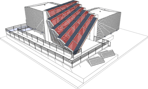
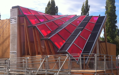
Building integration of photovoltaic (BIPV) modules is a key technology that integrated solar elements into buildings to generate electricity, to exploit sunlight for indoor illumination and thermal energy for heating or cooling application. We collaborate with Eni Spa, Powerglax Srl, Lumena AG and many other reference companies to develop the next generation of BIPV solutions. We are partner of the H2020 Ideas Project, in collaboration with the Trinity College of Dublin, the University of Ulster, the LEITAT Technological Center to develop an integrated solution for concentrating photovoltaic and thermal modules to enhance the electrical and thermal efficiency of buildings. In the field of BIPV we collaborate with the École nationale supérieure d’architecture de Paris-Malaquais and we participated to two editions of the Solar Decathlon Europe Competition.
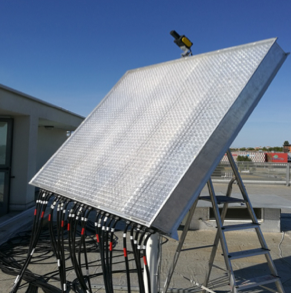
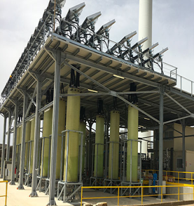
Solar energy harvesting involves not just the direct generation of electric energy from sunlight. Solar to fuel conversion can be based on the exploitation of natural processes like photosynthesis from vegetal species such as microalgae or plants. Microalgae biomass, in particular, is considered a potential feedstock for biofuel production and global CO2 sequestration. Sunlight is one of the most important factors in algae cultivation since it is the main driver in the chemical reactions during the photosynthesis process. We model with raytracing software the spectral light distribution inside photobioreactors (PBRs) and we develop solar light concentrators to collect and distribute sunlight in growth units. This activity is carried out in collaboration with Biosyentex Srl, Eni Spa and Compagnia Energie Rinnovabili Srl. Sunlight, indeed, can be used for any photosynthetic process; “indoor solar to food” conversion is a new challenging approach that consist in cultivating crops in controlled-environment such as shipping containers. Indoor farming avoids the use of pesticides and allow the cultivation of crops in harsh environments such as desertic areas where standard agriculture would not be possible.
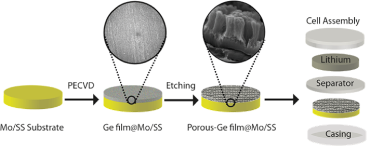
The intrinsic variability of the solar source leads to the development of energy accumulation strategies. The experience gained in the material science within the Sensor&Semiconductor Lab of the University of Ferrara led the Solar Energy Systems Laboratory to develop, in collaboration with Istituto Italiano di Tecnologia (Genova) and Fondazione Bruno Kessler (Trento) new materials to be used in the fabrication of next generation lithium-ion batteries. Due to the steady increasing demand for higher performance electronic devices and for the rising electric mobility market, it is required an increase of the actual specific energy of Lithium Ion Batteries (LIBs). This can be achieved increasing the gravimetric capacity of the electrodes, i.e. the amount of charge that can be stored per unit of mass of the active material. We developed nanoporous germanium anodes directly grown on a metallic current collector through a plasma enhanced chemical vapour deposition technique (PECVD). These anodes are able to perform hundreds of charge and discharge cycles at very high C-rates, retaining a stable capacity of more than 950 mAh/g even at currents as high as 5C (considering 1C as 1600 mA/g), which is 2,5 times the theoretical capacity of graphite. The main application of this technology is aero-space industry. The development of nanoporous germanium anodes has been funded by Italian Space Agency (projects ANGELS and GLITTERY).
Crystal Channeling Laboratory
The Crystal Channeling Laboratory is part of the Sensor&Semiconductor Lab of Ferrara University and of the Italian Institute for Nuclear Physics (INFN) – Ferrara Unit. Experimental condensed matter and particle physicists compose the research team, leading to the development of new technologies bridging solid state and high-energy physics.
In a crystal, atoms occupy well-ordered positions, resulting in peculiar effects as they are crossed by relativistic particle beams. One of the most interesting phenomena relies on channeling of ultra-high energy charged particle beams between the atomic planes of a bent crystal. Such effect results in beam deflection, which is typically achieved through conventional magnets, and find application in ultra-high energy particle accelerators, such as the Large Hadron Collider at CERN. Indeed, crystals might play a crucial role for the future developments of particle accelerators: differently from superconducting magnets, which require a huge amount of electric power and to operate at ultra-low temperature, bent crystals do not require any power source or cooling systems.

(left) Channeling of a proton beam inside a crystal; (right) Bent crystal used as primary collimator for the 7 TeV proton beam of the Large Hadron Collider @CERN.
Other than beam deflection and steering, the lattice structure can strongly influence the electromagnetic processes in oriented crystals, resulting in the enhancement of gamma radiation emission by ultrarelativistic electrons. This research activity is nowadays relevant to broad international communities, where availability of high-intensity gamma beams is demanded for applications spanning from nuclear physics to biology. In addition, the enhancement of electromagnetic processes can be exploited for the realization of compact electromagnetic calorimeter in high-energy physics.
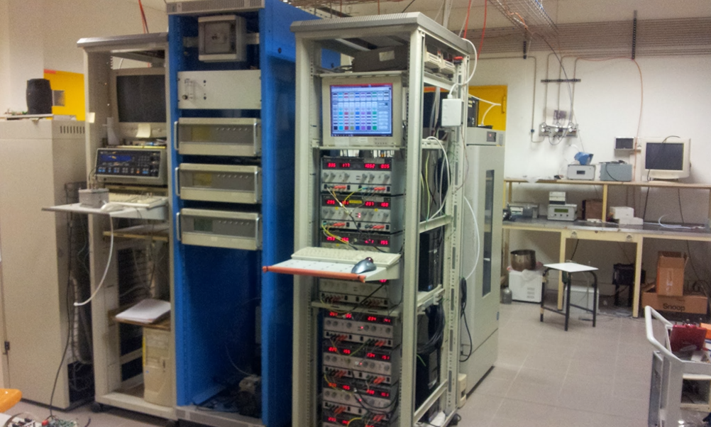
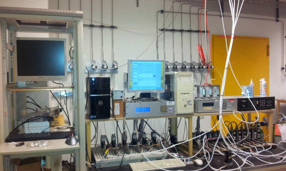
The manufacturing process of crystals is accomplished in a clean room environment, fully equipped with high-resolution x-ray diffractometers, a photolithographic line and interferometers.
The Ferrara team also participates to national and international collaborations, with experimental activities “on beam” in different international laboratories, such as CERN (Switzerland), SLAC (USA), MAMI and DESY (Germany), etc…, contributing to data analysis and Monte Carlo simulations.
The Crystal Channeling group has been part of several Europen projects (FP7: CUTE and ERC CRYSBEAM; H2020: PEARL, N-LIGHT and ERC SELDOM).
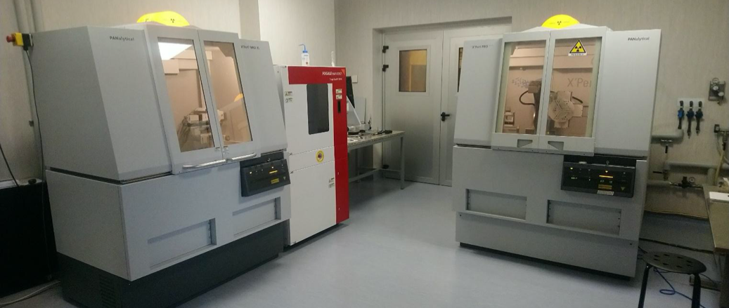
Crystal Channeling Lab Clean Room: High-energy resolution X-ray diffractometers.